Optoelectronic oscillators (OEOs) have emerged as indispensable tools for generating low-phase-noise microwave and millimeter-wave signals,
Our low-loss TSV and RDL can be readily used as key components in the development of interposer systems, and well support the transmission of high-frequency signals, which is a big step
Two invited papers cover important history and developments of low loss silicon nitride waveguides, the Photonic Damascene process and the TriPleX process.
This passive alignment concept enables accurate and simple plug-in of optical and optoelectronic elements, into a PCB. The concept is based on established PCB manufacturing processes, which is
We propose innovative polarization-insensitive optical switch fabrics on the 220-nm SOI platform, featuring polarization-insensitive switch elements, polarization-insensitive waveguide crossings, and
In particular we focused on devices that closely coupled electronics with photonics for low-loss data transmission, in order to realize multiple order-of-magnitude gains in performance and
The research status, technical challenges and development trend of devices, chips and integrated technologies of typical IC and optoelectronic chips
Waveguides fabricated in high-index-contrast material systems offer very strong light confinement compared to that achieved in low-index-contrast material systems. A core layer of
The low-loss and high-fidelity programmable transformations of the integrated processor showed its potential advantages for many-boson quantum
The integration of microelectronic and photonic circuits on a single silicon chip for high-speed and low-power optoelectronic technology
This chapter will review fundamentals and design guides of optical waveguides, including state-of-the-art and challenges, fundamental theory and design methodology, fabrication techniques,
Here, we propose a strategy to achieve ultralow-loss grating couplers by using unidirectional guided resonances (UGRs), suppressing the
The length variation associated with standard cleaving of III–V optoelectronic chips is a major source of loss in the integration with the micron
We have developed novel optoelectronic packages and optical transmission system using an optical connector with an external optical waveguide to achieve low-loss chip-to-chip optical
In this work, a low loss silicon photonic interposer for the 2.5D / 3D optoelectronic integration is fabricated including 1-layer of metal-1 (M1) wiring for the optical modulator, 1-layer of
This type of oscillator shows promise in generating low-noise high-frequency microwave signals, which are crucial for applications such as 5G communication, test and measurement equipment, and
In Section 1, we introduce the background and significance of the development of silicon-based optoelectronic heterogeneous integration chips. In Section 2, we
Designed to guide light vertically with minimal loss, these vias can be filled with low-loss optical materials or air. They are fabricated using precision etching and deposition techniques to ensure
Optoelectronic integrated circuit (OEIC) technology has attracted considerable research attention. Studies have achieved numerous
Optoelectronic integration thus presents challenges in a number of different areas such as materials, devices, processing and packaging, depending on which components are integrated. For discussing
The integration of low-capacitance photodetectors can largely eliminate the dissipation from electronic circuits used for receiver amplifiers, in what we will call “receiverless” or “near-receiverless”
Guiding of light is fundamental to optical communication and integrated photonic circuits. To confine the propagating electromagnetic waves and guide them with low loss, the use of select
We present two heterogeneous integration techniques that enable high-density electrical and optical I/O connections, utilizing adiabatic coupling
This chapter will highlight the challenges specific to optoelectronic device packaging and will explore some new and exciting packaging concepts that promise to satisfy reliability requirements, preserve
To achieve low loss U-bends with small footprint, we utilize the Euler bend geometry previously demonstrated on silicon and GaAs platforms. We analyze the gain properties of the devices by
Request PDF | Low-loss through silicon Vias (TSVs) and transmission lines for 3D optoelectronic integration | The optoelectronic hybrid integration based on co-package has attracted
We present two heterogeneous integration techniques that enable high-density optical I/O connections, utilizing adiabatic coupling between on-chip silicon nitride (SiN) wave-guides and package-level
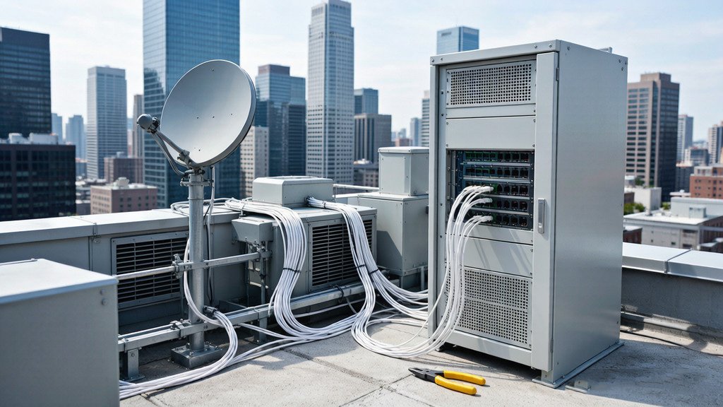
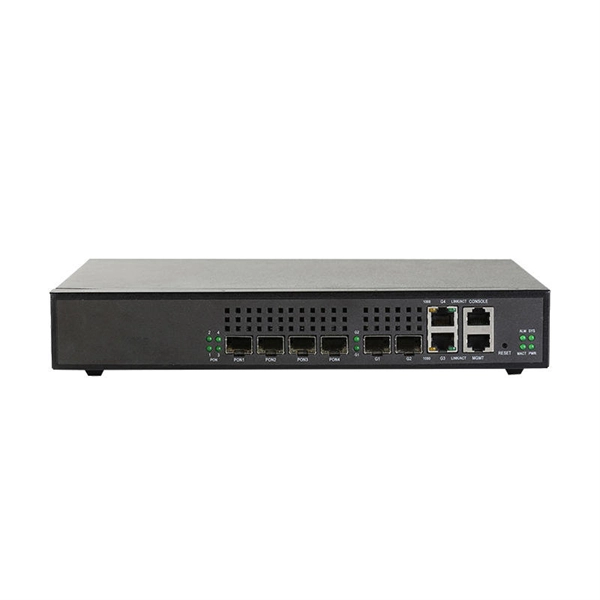
Contact us for competitive quotes on any of our power communication and smart grid products
Get a Quote